Dai Nippon Printing Establishes First Overseas R&D Hub in the Netherlands
Expansion in advanced materials research in semicon enabled by partnerships with Dutch High Tech Ecosystem
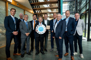
Japanese innovation leader Dai Nippon Printing Co., Ltd. (DNP) has announced the establishment of its first overseas research and development hub in partnership with TNO, or the Netherlands Organisation for Applied Scientific Research, at the High Tech Campus Eindhoven (HTCE). This marks a significant milestone in DNP’s global expansion strategy and a major boost to the Netherlands’ High Tech ecosystem.
DNP collaboration with TNO and Photonic Integration Technology Centre
The new R&D center will serve as a strategic base for DNP’s advanced materials research, with a focus on next-generation semiconductor-related technologies. As part of the work, DNP and TNO will collaborate with the Photonic Integration Technology Centre (PITC) to conduct a three-year joint research program. This move underscores the Netherlands’ growing reputation as a global hub for high tech innovation, particularly in the fields of photonics, semiconductors, and advanced materials.
World-class innovation infrastructure and collaborative ecosystem
DNP’s decision to locate in Eindhoven was driven by the region’s world-class innovation infrastructure and collaborative ecosystem. The strategic partnership is aimed at developing cutting-edge technologies that address global challenges in energy efficiency, data processing, and sustainable manufacturing. The partnership and its new R&D hub will focus on advancing Co-Packaged Optics, a key technology for enabling the development of next-generation semiconductors.
“We are very pleased with this collaboration with TNO/PITC”, said Hideto Sakata, Corporate Officer, Head of Technology and R&D Division at DNP. “We expect this collaboration will elevate our global technology strategy and contribute to sustainable digital infrastructure. By establishing a new R&D centre in HTCE, the smartest global high-tech cluster, we will accelerate open innovation and advanced technologies such as integrated photonics.”
A thriving semiconductor ecosystem
The new hub complements the Netherlands’ thriving semiconductor and high tech materials science sectors, which include institutions such as ASML, TU Eindhoven, and a vibrant network of SMEs and research institutes.
The Netherlands has transformed the global landscape of semiconductor technology, highlighted by the fact that it is one of three countries in the world to have a complete semiconductor value chain within its borders. Notably, 85% of all chips globally use Dutch semiconductors equipment in their design, development and manufacture.
Dutch government support
The investment was supported by the Netherlands Foreign Investment Agency (NFIA), its Tokyo-based team, and the regional development agency Brabant Development Agency (BOM). Their coordinated efforts assisted in DNP navigating the Dutch innovation landscape and connecting with key partners.
With this move, DNP joins this growing list of international companies choosing the Netherlands as a base for innovation, reinforcing the country’s position as a gateway to Europe and a leader in collaborative, cutting-edge R&D.
Source: DNP Printing & TNO
4 September 2025